
")
")
FINEPLACER® sigma
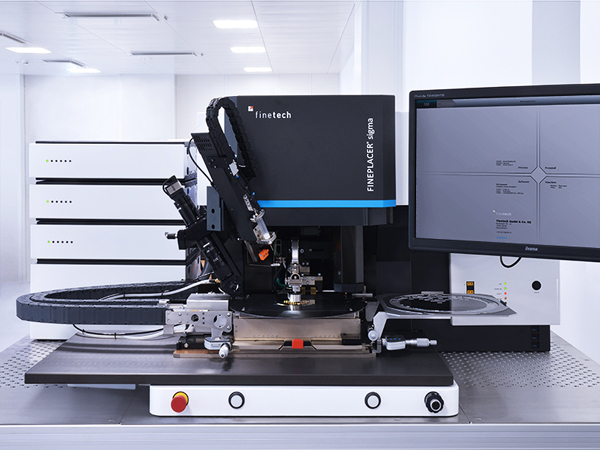
Semi-automated Sub-Micron Bonder
The FINEPLACER® sigma combines sub-micron placement accuracy with a 450 x 150 mm working area and bonding forces up to 1000 N. The system is ideal for all types of precision die bonding and flip chip applications at chip and wafer level. This includes complex 2.5D and 3D IC packages, Focal Plane Arrays (i.e. image sensors), MEMS/MOEMS, and more.
Placing small devices on large substrates is made possible by the FPXvisionTM optical system design. With this alignment system, the smallest structures at the highest magnification can be viewed across the entire field of view. Moreover, FPXvisionTM introduces pattern recognition to a die bonder with manual alignment.
The FINEPLACER® sigma embraces all features of an assembly and development platform capable of handling an unlimited spectrum of applications and prepared for future technologies.
Highlights*
- Sub micron placement accuracy
- Supports 300 mm wafers
- Bonding forces up to 1000 N
- FPXvisionTM - high resolution for all magnifications
- Software guided alignment verification
- Touch screen GUI
- Modular design for flexible configurations
Technologies
- Thermocompression bonding
- Thermo- / ultrasonic bonding
- Soldering (AuSn / eutectic, Indium, C4)
- Adhesive technologies
- ACF/ ACP bonding
- UV / thermal curing
- Cu / Cu bonding, copper pillar bonding
- Precision vacuum die bonding
- Sintering
- Micro mechanical assembly
Applications
- Wafer level packaging (FOWLP, W2W, C2W)
- 2.5D and 3D IC packaging (TSV)
- Multi chip packaging (MCM, MCP)
- Flip chip bonding (face down)
- Precision die bonding (face up)
- µLED and µLED array bonding
- Optical package assembly
- MEMS/MOEMS packaging
- Sensor assembly
- Glass-on-glass, chip-on-glass, chip-on-flex